Inorganic Core Substrate for Semiconductor Packaging
Advancing TGV (Thorough Glass Vias) processing
The inorganic core substrate is designed for high-performance, high-density semiconductor packages. We are advancing the development and supply of large glass core substrates and large glass-ceramic substrates, GC Core™ —by leveraging TGV processing with a general-purpose CO₂ laser and laser modification and etching techniques.
What Is an Inorganic Core Substrate?
-
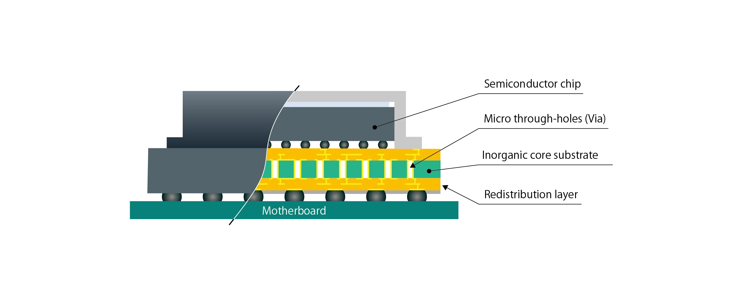
An inorganic core substrate is an alternative to conventional organic substrates that connect semiconductor chips to external circuits. Instead of using organic materials like those found in glass epoxy substrates, inorganic core substrates employ inorganic materials to deliver superior electrical properties, enhanced rigidity, and exceptional flatness. NEG is advancing this technology by developing both glass-ceramic core substrates, GC Core™ and glass core substrates.
| Organic core substrate | Inorganic core substrate | |
|---|---|---|
| Electrical properties | Inferior | Superior |
| Rigidity | Low | High |
| Flatness | Inferior | Superior |
-
TGV processing system
-
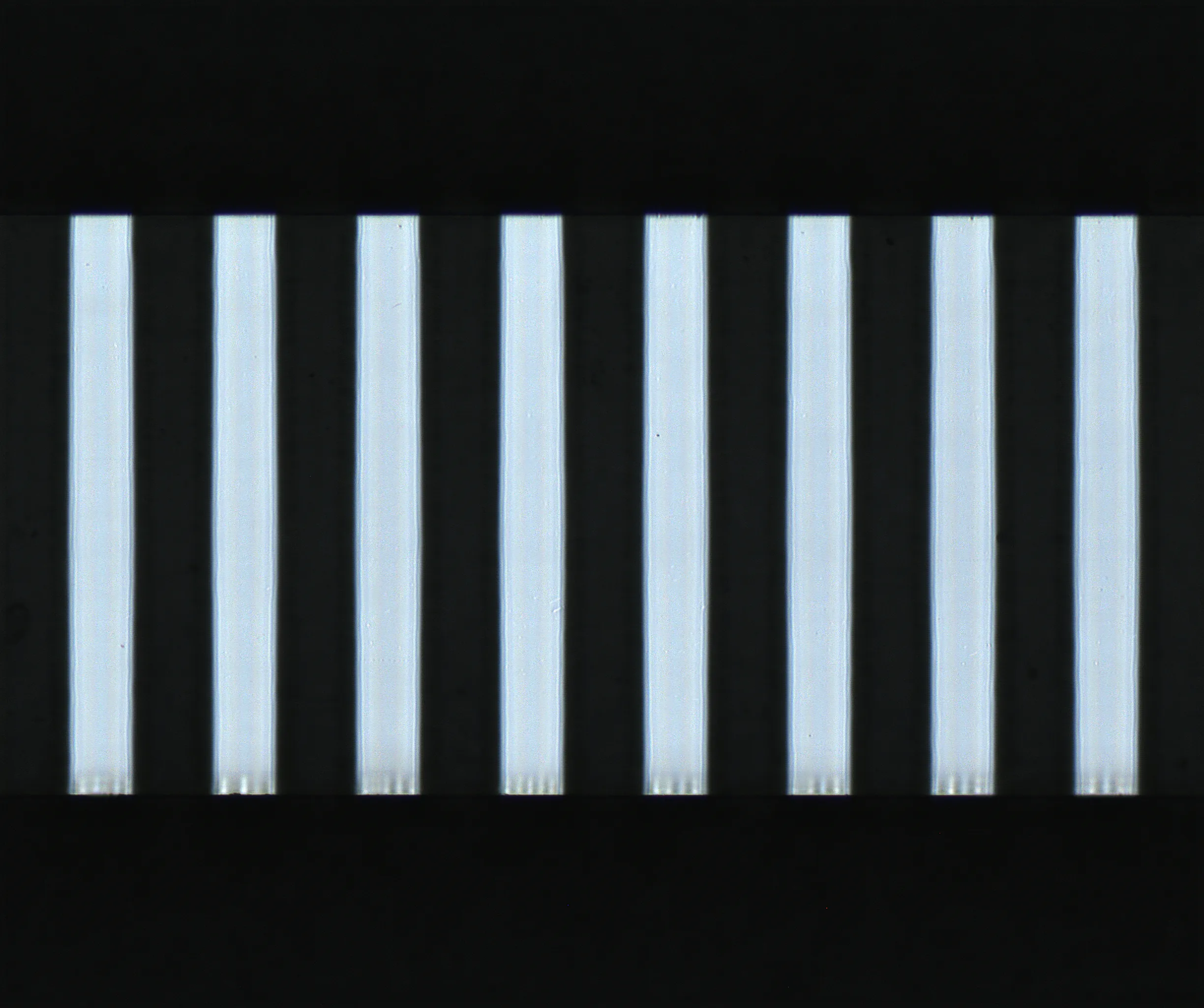
CO2 laser proceessing
Characteristics
Direct laser drilling of vias in glass
Benefits
Fewer steps, high-speed processing, compatible with PCB laser processing machine -
Laser modification and etching
Characteristics
Laser irradiation modifies the glass, enabling selective etching to form vias
Benefits
Capable of processing TGVs with small diameters and narrow pitches
Damage resistance of the etching surface
Advantages of Our Inorganic Core Substrate
-
Material selection and substrate supply optimized for TGV processing
For inorganic core substrates, achieving crack-free TGV processing and scaling up to larger substrate sizes are essential. We offer both material selection optimized for TGV processing—including general-purpose CO₂ laser and laser modification and etching techniques—and supply of large substrates suitable for these advanced processes. -
Core substrate selection focused on thermal design
Thermal management is critical in semiconductor packaging to ensure reliability. In addition to our glass-ceramic core substrates, we are expanding our glass core substrate offerings, enabling us to provide core substrates with coefficients of thermal expansion precisely tailored to meet specific thermal design requirements. -
Extensive experience from material selection to processing
With years of experience supplying components for the semiconductor industry, we excel from material selection through final processing. This expertise allows us to propose core substrates with optimized dielectric properties that meet the unique demands of your applications.
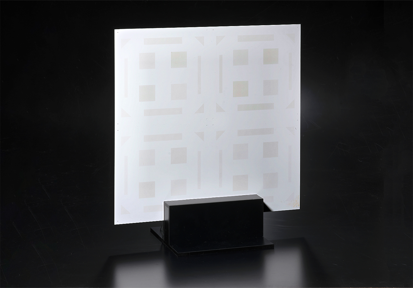
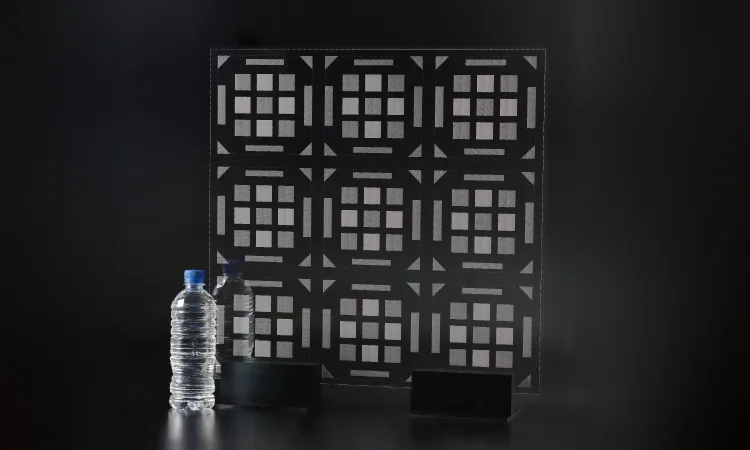
Glass-Ceramic Core Substrate GC Core™
-
By adjusting the composition and mixing ratio of glass and ceramics, this core substrate achieves a balance of key properties, including dielectric properties, coefficients of thermal expansion, and strengths.
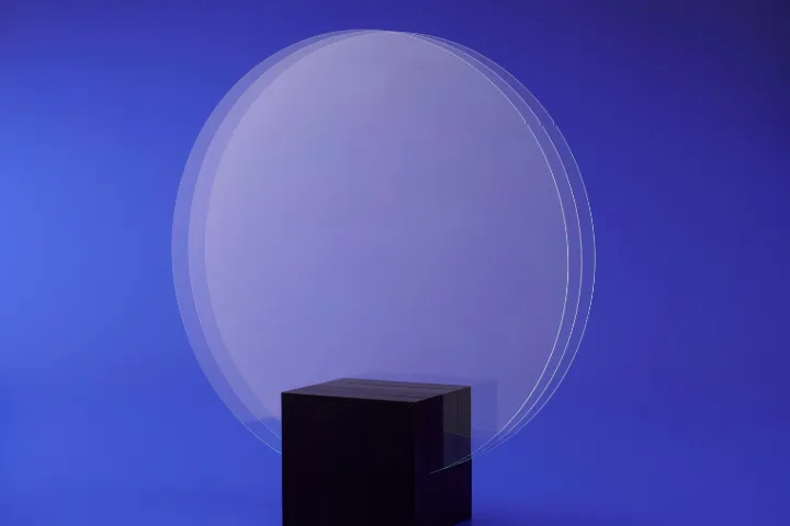
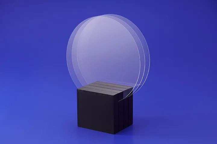
A large substrate size (515×510mm) has been developed for next-generation semiconductor packages.
-
Features
・Low dielectric constant, high expansion, and exceptional strength -
・Customizable to meet specific application requirements
| Type | Low dielectric constant type | High expansion type | High strength type | |
|---|---|---|---|---|
| Product code | GCC-1 | GCC-2 | GCC-3 | |
| Dielectric loss tangent | 2.45 GHz | 0.0013 | 0.0002 | 0.0004 |
| 40 GHz | 0.0016 | 0.0004 | 0.0007 | |
|
Dielectric constant |
2.45 GHz | 3.9 | 7.0 | 7.9 |
| 40 GHz | 3.8 | 6.8 | 7.6 | |
| Coefficient of thermal expansion (ppm/°C) | 6.1 | 8.9 | 7.4 | |
| Bending strength (MPa) | 150 | 260 | 340 | |
Glass Core Substrate
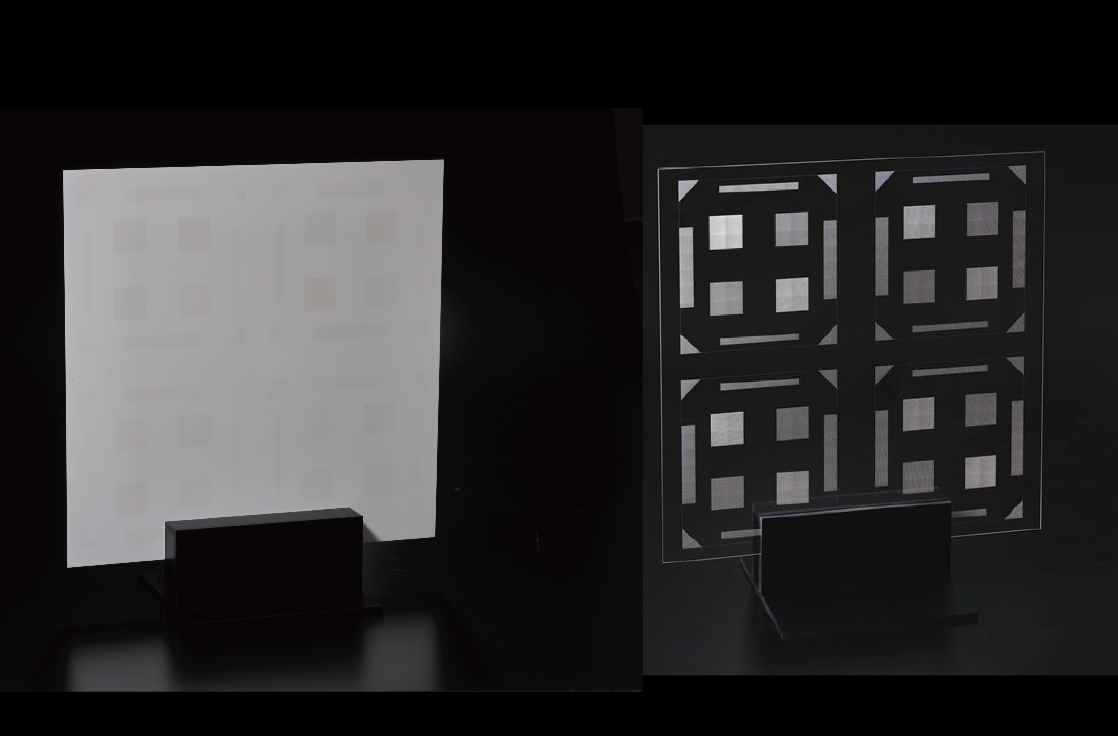
Compared to organic material-based substrates like glass epoxy substrates, this core substrate offers superior flatness, smoothness, and rigidity, making it well-suited for larger sizes. We offer materials and substrates suitable for TGV processing using laser modification and etching and CO₂ lasers. Since 2020, we have been engaged in the development of glass materials and the provision of samples, and have successfully developed new materials optimized for laser modification and etching.
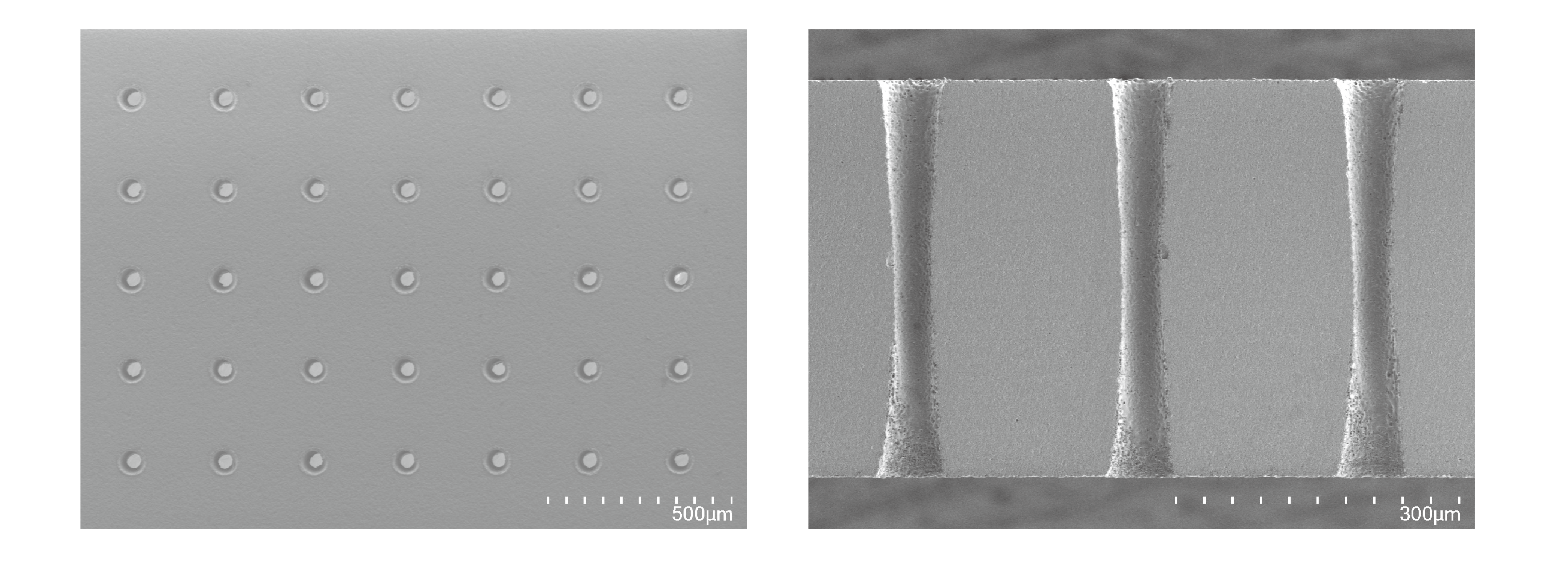
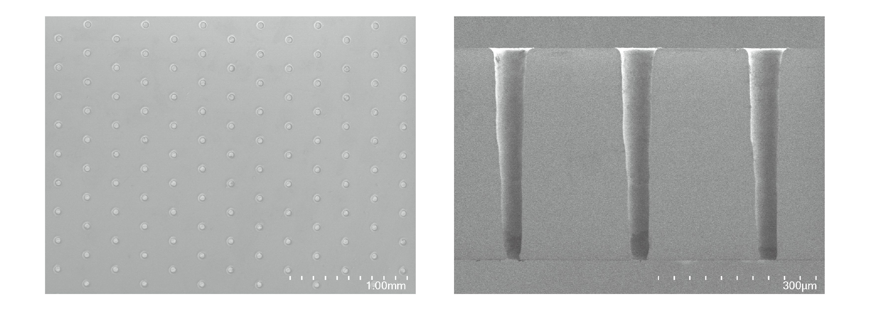
We are now able to provide large-size samples (515 × 510 mm) of glass core substrates with TGV processing.
(substrate thickness 0.4 mm, hole diameter Φ50μm)

(Substrate thickness 0.5 mm, hole diameter Φ90μm)
Key Features
-
Improved Productivity
・Selection of materials optimized for TGV processing
・Availability of large core substrates -
Excellent Reliability
・Reduced dimensional changes and warping under high temperature and humidity conditions
・Suitable for fine-pitch wiring and high-density packaging
When contacting us, please select “Glass Wafer for Supporting Semiconductors” from the dropdown menu.
Event Information
We will be exhibiting at the following events.